 A Country That Cannot Investigate Itself Cannot Govern Itself
  Thai Princess Kept Alive Artificially For More Than Three Years Dies
  Indie Film Causes Consternation Among Overseas Chinese
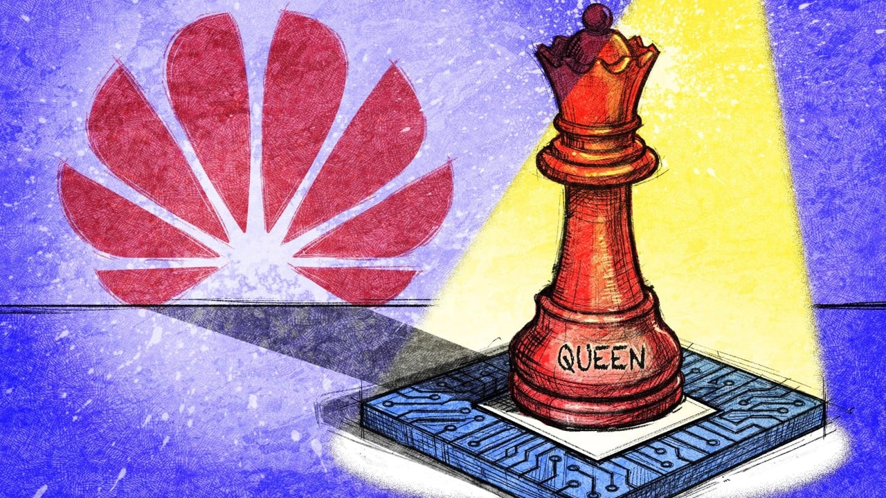
 The head of Huawei Technologies’ secretive semiconductor business – widely dubbed the company’s “chip queen” – had been out of the public view since 2019, when Washington severed the Chinese company’s global access to advanced technology, including semiconductors.
Her retreat into the background became a symbol of Huawei’s battle for survival. That all changed last month on a global academic stage in Shanghai – the IEEE International Symposium on Circuits and Systems.
Advertisement
It was there that He introduced the “Tau (τ) Scaling Law”, which Huawei claimed could achieve transistor densities equivalent to the cutting-edge 1.4-nanometre process by 2031 – all without the need for advanced extreme ultraviolet (EUV) lithography machines out of reach due to US sanctions.

Redefining ‘advanced’
For half a century, the electronics industry treated Moore’s Law – the principle that the number of transistors on a chip doubles roughly every two years – as gospel. But as silicon structures approached atomic limits, geometric scaling was yielding diminishing economic returns and hitting an architectural brick wall.
Don't Miss:
-
Why SpaceX may not be a model for Chinese companies to copy
-
How to say ‘tomato sauce’ in Cantonese? A Miss Hong Kong hopeful sparks culture debate
-
Chinese team flags life-threatening ‘glaring weakness’ in Nasa’s Artemis programme
-
India military transport plane crash kills 5
-
Police seize HK$7.2m of drugs, target syndicate recruiting using online gaming