
 Bangladesh’s Hill Country Needs Dialogue, Not More Bureaucracy
  National Press Club Bans Reporters While Protesting Trump’s Banning of Reporters
  ICIJ journalist Micah Reddy freed after 4 days in secretive Djibouti custody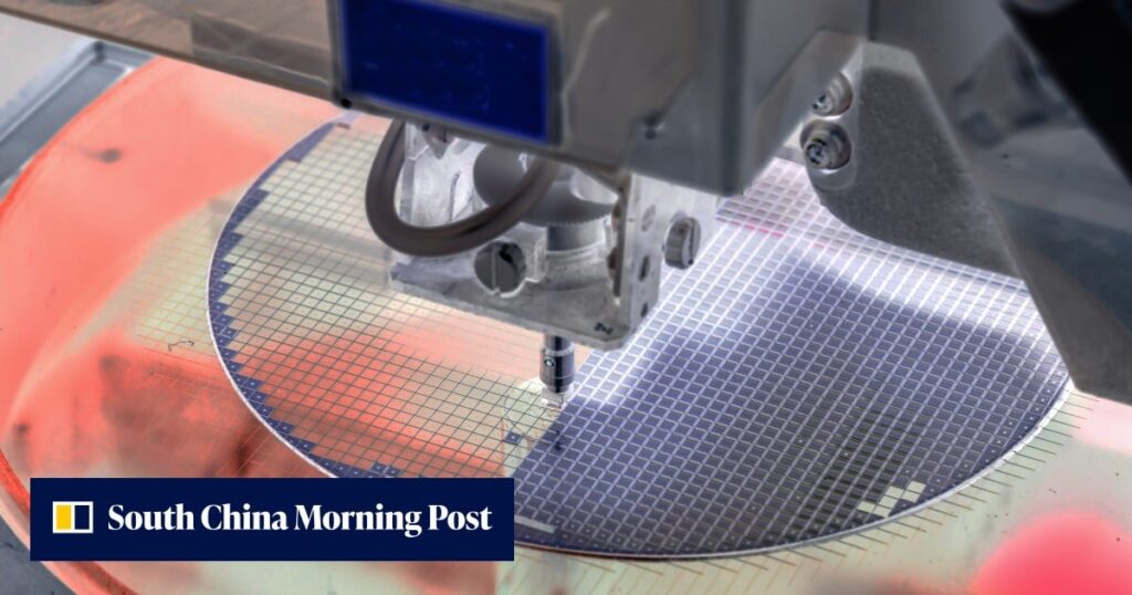
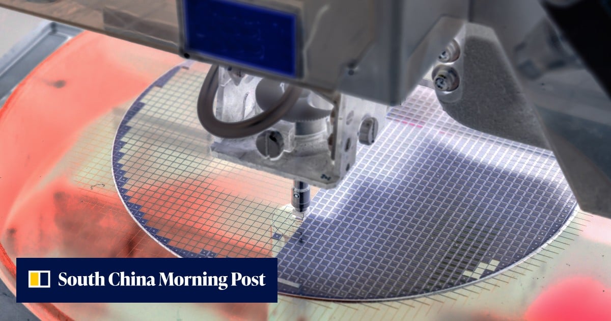
Chinese storage makers, long known for packaging chips into modules, have been moving up the value chain into wafer-level operations, with the latest firm to make the jump investing 4.5 billion yuan (US$672 million) in an advanced packaging project.
The sum, which Shanghai-listed Biwin Storage Technology will pour into the third phase of its advanced packaging and testing project in Dongguan, in southern China’s Guangdong province, will exceed the 3.09 billion yuan it put into the first two phases combined.
The project, including the first two phases, had yet to generate mass production revenue, as it was still undergoing customer sampling, process verification and small-batch production, according to Biwin’s stock filing on Tuesday. The company estimated that the facility’s monthly capacity would more than triple to 10,000 wafers by the end of 2027, according to the filing and earlier investor meetings.
The gamble marks a move into more sophisticated wafer-level technologies, as Biwin already operates a traditional memory and system-in-package, or SiP, packaging base in Huizhou, also in Guangdong, where it sources chips from external suppliers.
Don't Miss:
-
Hong Kong pledges lenient approach on 10-12 hours of civil service family leave
-
Italy’s Colosseum closes after worker dies in accident
-
China hawks grumble over Trump’s lavish welcome planned for Xi state visit
-
Why younger Filipinos are warming to China despite maritime tensions
-
As Chinese carmakers diversify beyond CATL batteries, Beijing warns of market overreaction